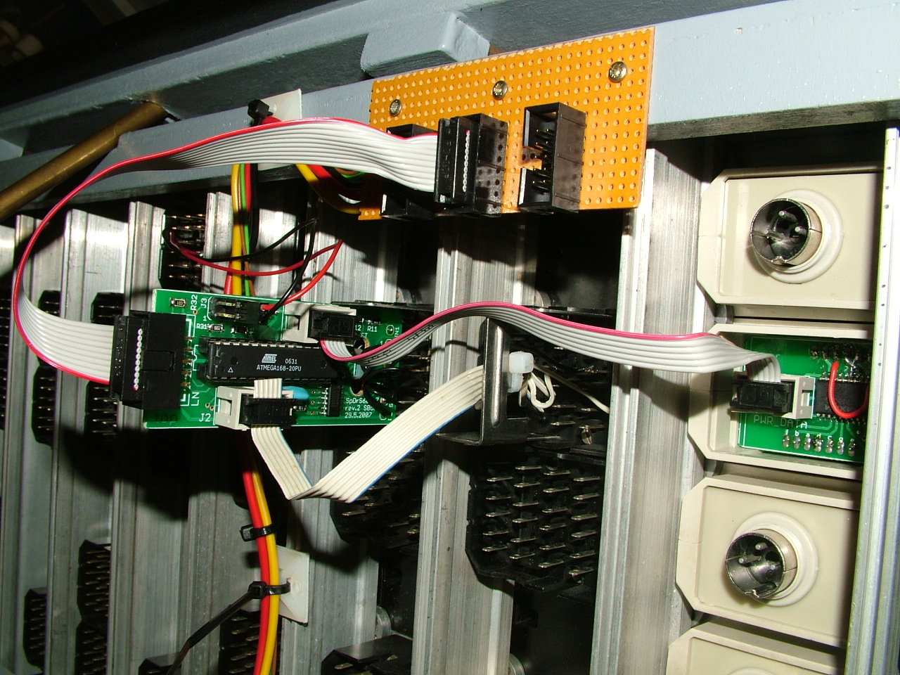
IO boards for panelsHardwareThe following two boards are under test. They have in common that they are ment to be used for a prototypical panel and can connect to train number displays via SPI. SpDrS60This board is designed to be fixed under a single prototype SpDrS60 panel module. It is capable of driving 12V or 24V light bulbs and sample buttons that are connected to 12V or 24V.
A second generation of this board is manufactured. Boards are currently in use for "Stefanswiesen" and intended for "Delthin". The design works more or less. Software update with all 13 boards on the net does not work and sometimes a single board does not boot on power up of the system. There is a default pin usage for SpDrS60. List of connectors:
IO board with 60 TTL level linesThis board is designed to interface with transistor based panel electronics for the Michelstadt
The first board and a second batch of three boards are currently in use. The operation in Rastede 2008 was promising but showed erratic behaviour. A debouncing algorithm is needed to avoid a message shower. But the message shower is probably triggered by bad electric design in the system or the board. More debugging will be done. SoftwareBoth boards will use the same software. A configuration option decides over the pin usage which is both hardware dependant and about the decision wether to use the SPI processor pins for connection to a chain of train number displays or digital IO. For digital IO, the software uses a test mode protocol that is used by Uhlenbrock to test their own panel boards. This protocol is based on the LNCV programming. For access to the train number displays, the defined message based on OPC_PEER_XFER as defined by Digitrax. For configuration the SV programming protocol is used. See this table of SVs. Software update over LocoNet is available with the IPL protocol using a BootLoader. LocoNet message bit to connector pad assignmentThere is a little Java application that helps testing the IO functionallity of the boards. Mode Configuration
Outputs
Inputs
Alternative ZN-only softwareSoftware can be found on the subversion server in this directory This software supports only ZN displays and no IO pins. Instead of using the single hardware SPI interface inside the AVR, we use software that bit-bang the data stream to the displays. This way six chains are supported. The maximum number of displays per chain is defined to be six, this is a software constant, that could changed, but it is not configurable at runtime. The following table shows the assignment of display chains number and pin function to pins on the connector. First row are the System Variable numbers where you configure the address of the display that is wired directly to the processor. Next display behind that in the same chain has the following two SVs. The background color just highlights the border between the pin groups that form individual interfaces, each is the starting point of one chain of displays. ZN pins
FREMO Interlocking Webmaster
Bernd Wisotzki und
Stefan Bormann.
Eine Verantwortung für Fehler und Unterlassungen wird ausdrücklich abgelehnt. Responsibility for errors and ommissions is expressively rejected
Site hosted by:
|
|||||||||||||||||||||||||||||||||||||||||||||||||||||||||||||||||||||||||||||||||||||||||||||||||||||||||||||||||||||||||||||||||||||||||||||||||||||||||||||||||||||||||||||||||||||||||||||||||||||||||||||||||||||||||||||||||||||||||||||||||||||||||||||||||||||||||||||||||||||||||||||||||||||||||||||||||||||||||||||||||||||||||||||||||||||||||||||||||||||||||||||||||||||||||||||||||||||||||||